/cdn.vox-cdn.com/uploads/chorus_asset/file/24016885/STK093_Google_04.jpg)


/cdn.vox-cdn.com/uploads/chorus_asset/file/24808816/Starfield__The_Settled_Systems___Supra_Et_Ultra_____Starfield__The_Settled_Systems___Supra_Et_Ultra_2023_7_25_94252.263_1440p_streamshot.png)


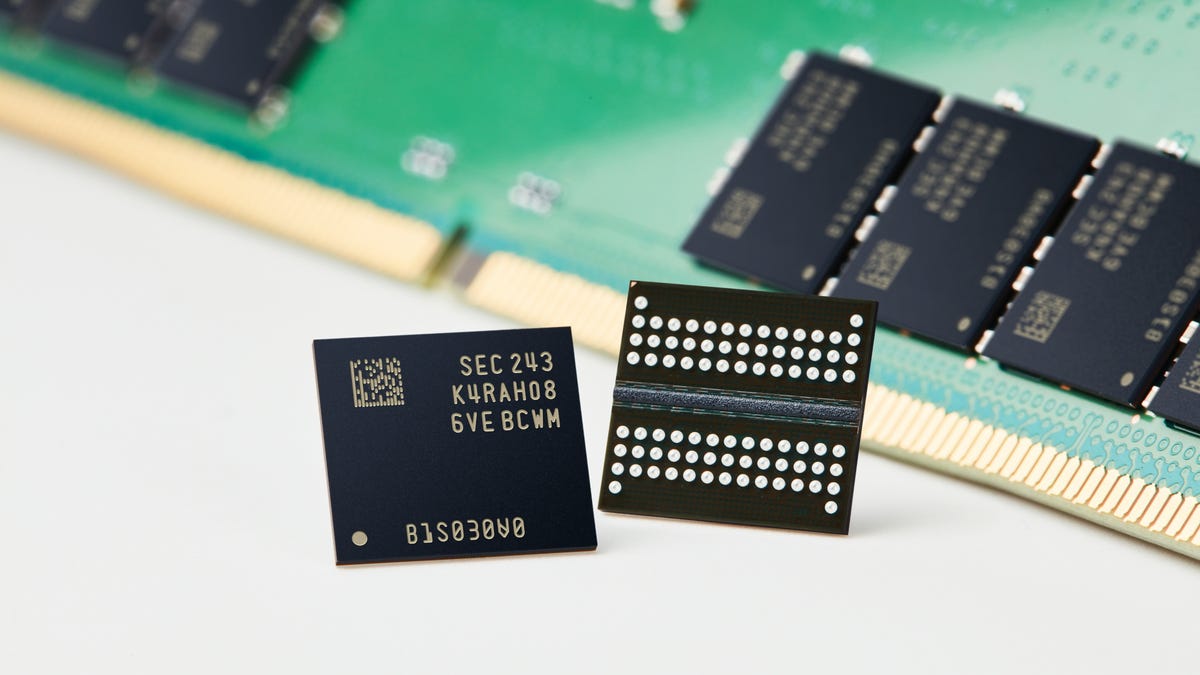
Samsung said on Thursday it has begun mass production of its Double Data Rate 5 (DDR5) DRAM made from a 12-nanometer (nm) class process node. The tech giant had announced the development of 16GB DDR5 DRAM in December last year.
The start of mass production of 12nm DRAM, which makes it the most advanced DRAM available, at a time when the memory chip industry is going through a recession, shows that Samsung, the world’s largest memory chipmaker, is continuing its leadership. intends to maintain. more in the field.
According to Samsung, the new chip, compared to the previous generation, has reduced power consumption by 23%, while increasing its wafer productivity by 20%, meaning that 20% more chips can be produced from the same wafer. can be done because the chip is smaller than that. former generation.
The tech giant said that the low power consumption from 16GB of DDR5 DRAM will allow server and data center operators to reduce their energy consumption and carbon footprint.
The chip has a maximum speed of 7.2Gbps, which means it can process 60GB in about a second, and is aimed at data centers, AI and new computing applications.
The 12nm node was achieved thanks to Samsung’s use of a new High-K material that allows the chip to accurately differentiate differences in data signals.
The DRAM has already been verified for compatibility with AMD in December and Samsung said it is currently collaborating with more global IT companies.
